Difference between revisions of "83Plus:Overclocking"
(Add specifics for overclocking) |
m (Hopefully fix characters) |
||
| Line 12: | Line 12: | ||
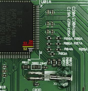
[[File:TA1 ASIC overclock.jpg|350px|thumb|right|Image of the TA1 ASIC highlighting the relevant pins. Note the silk-screened pin 51 label.]] | [[File:TA1 ASIC overclock.jpg|350px|thumb|right|Image of the TA1 ASIC highlighting the relevant pins. Note the silk-screened pin 51 label.]] | ||
| − | Each successive CPU speed mode enables more resistors in parallel. In mode 0, only R08D is used; in mode 1, R07D is in parallel with R08D. On my (DrDnar's) calculators, I get R08D | + | Each successive CPU speed mode enables more resistors in parallel. In mode 0, only R08D is used; in mode 1, R07D is in parallel with R08D. On my (DrDnar's) calculators, I get R08D ≈ 1.8 k? and R07D ≈ 1.2 k?. To overclock CPU speed 1 to ≈ 20.4 MHz, replace R07D with an 820 ? resistor. 20 MHz is pushing the limits of what the flash chip is spec'd for, so consider instead 910 ? for ≈ 19 MHz, or 1 k? for ≈ 18 MHz, which should hopefully be safe for all calculators. |
Revision as of 17:14, 7 May 2020
The TI-83+SE, TI-84+, TI-84+SE, and TI-84+CSE can all be overclocked. The TI-83+SE had special solder pads to enable overclocking, but the TI-84+ series lacks them.
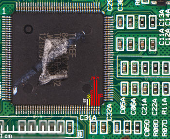
The TI-84+CSE and older TI-84+/SEs use the TA3 ASIC (port 15 reads 45h), pictured on the right. Pins 67-72 on the TA3 connect to an external RC tank circuit. The calculators have 4 CPU speed modes, which were originally supposed to be 6, 15, 20, and 25 MHz; production calculators only have 6 and 15 MHz modes. The four red pins correspond to the four CPU speed modes.
To enable speeds 02 and 03 on the TA3, add resistors on pins 70 and 71. The calculator seems unstable above 22 MHz, which suggests that TI didn't implement the 20 MHz mode due to resistors not being accurate enough (some calcs might get a particularly bad resistor and end up being more like 23 MHz for the resistor value that should give 20 MHz). The TA1 ASIC is a reduced pin count design and appears to lack the pins for the 02 and 03 CPU modes.
Each successive CPU speed mode enables more resistors in parallel. In mode 0, only R08D is used; in mode 1, R07D is in parallel with R08D. On my (DrDnar's) calculators, I get R08D ≈ 1.8 k? and R07D ≈ 1.2 k?. To overclock CPU speed 1 to ≈ 20.4 MHz, replace R07D with an 820 ? resistor. 20 MHz is pushing the limits of what the flash chip is spec'd for, so consider instead 910 ? for ≈ 19 MHz, or 1 k? for ≈ 18 MHz, which should hopefully be safe for all calculators.

